CRT Calculators · Volume 5
Theory of Operation: The HP 9100 and the Others
The Friden showed what could be done with a delay line, four counters and a tube. The other CRT calculators took different roads. Hewlett-Packard built a small computer with a read-only memory and microcode, the Victor 3900 put everything on MOS chips, the Wyle drew in curves from a spinning disk, and the later Fridens shrank the 130 into integrated circuits. This volume takes them in turn.
5.1 The HP 9100A: a calculator built like a computer
The primary source is the HP Journal of September 1968, in which Tom Osborne described the hardware and Dave Cochran the internal programming, with the detailed catalogue entry of Trinity College Dublin and Osborne’s own account of the project.
5.1.1 The logic
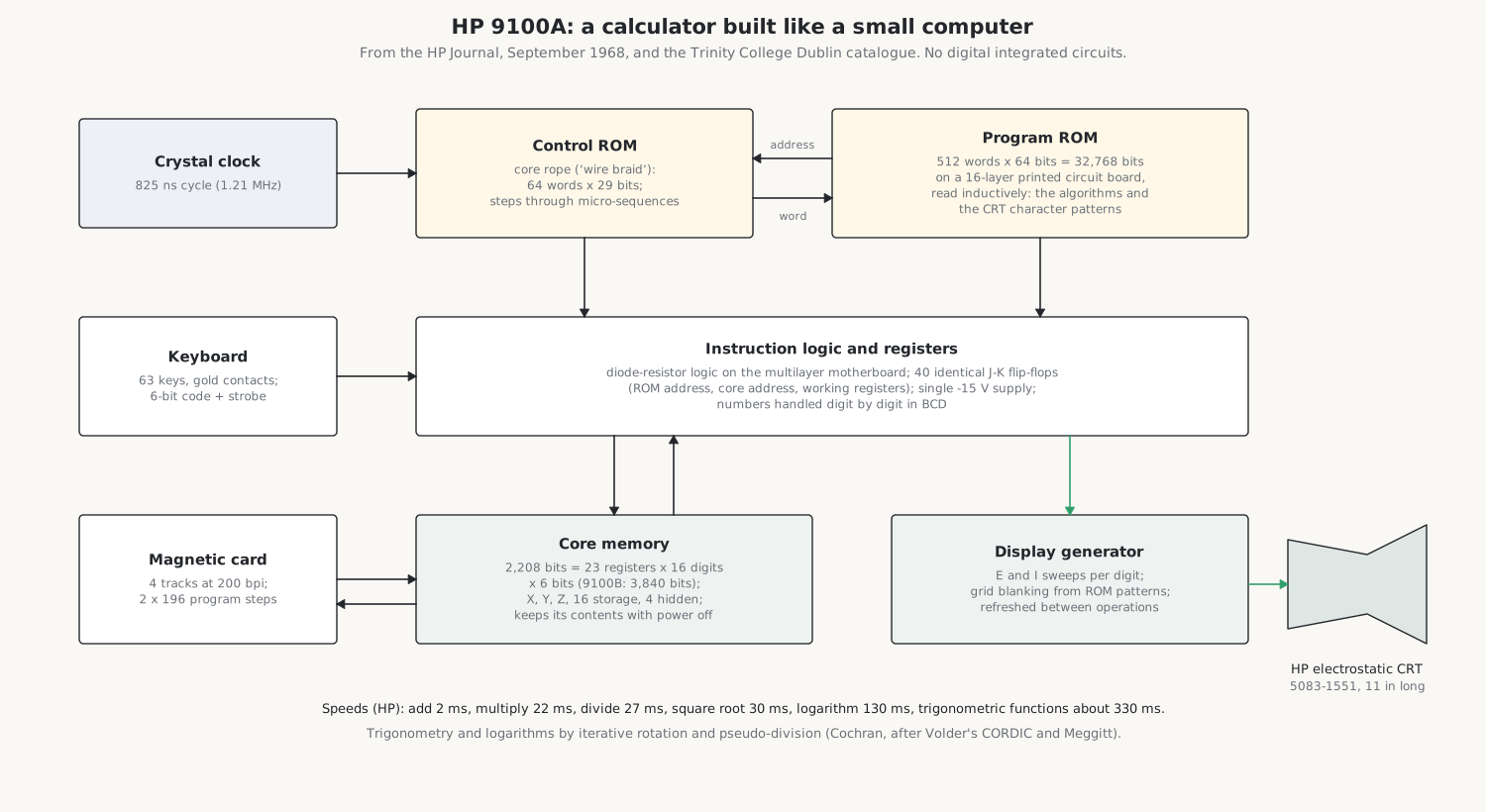
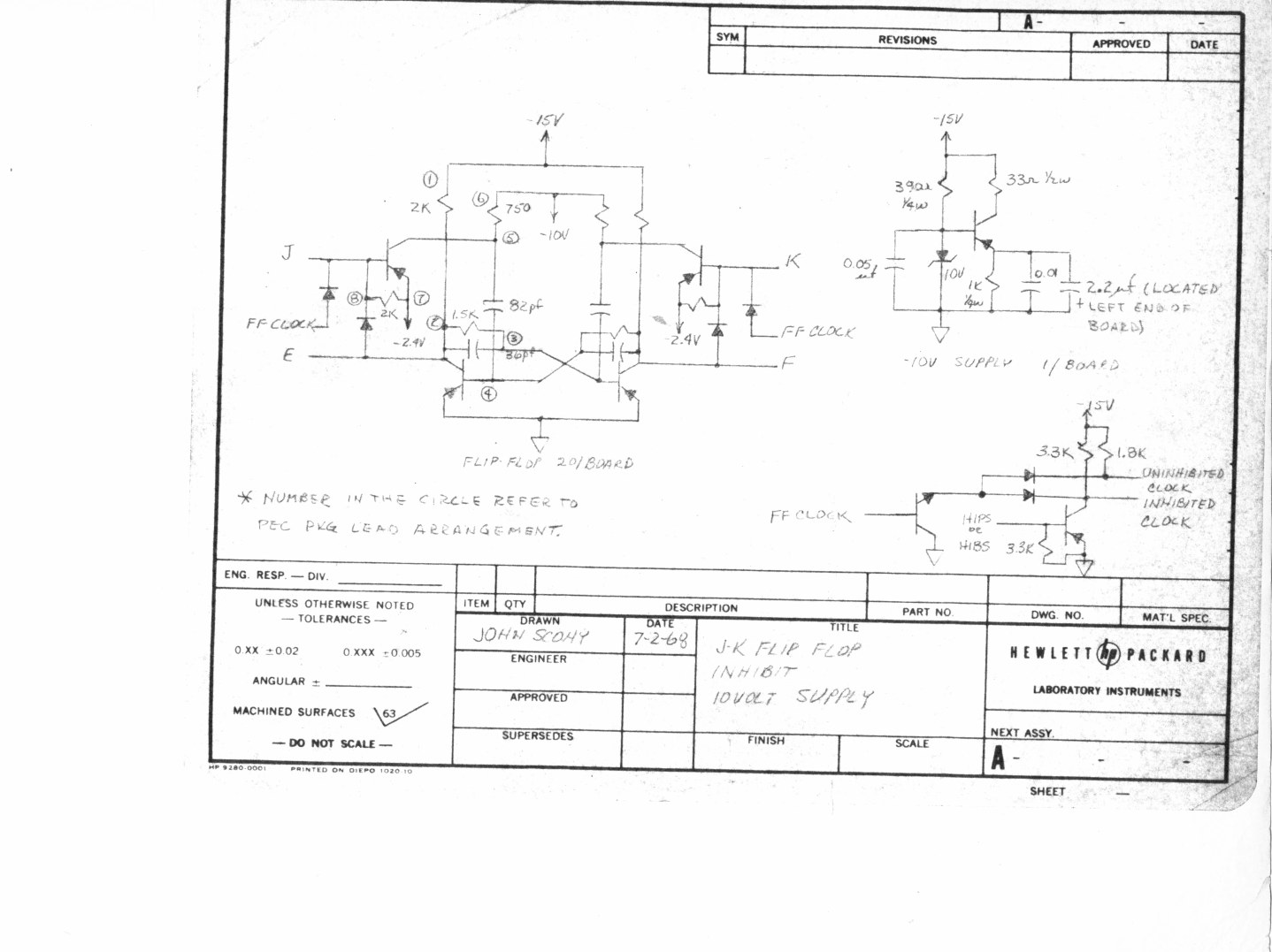
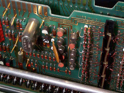
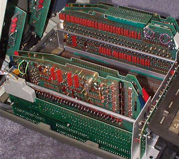
The 9100A contains no digital integrated circuits. Its logic is diode-resistor gating on a multilayer motherboard, with 40 identical J-K flip-flops on two boards, all run from a single −15 V supply (every circuit works from −13.5 to −16.5 V). The flip-flop is Osborne’s own design, patented as US 3,566,160: a race-free J-K flip-flop with a noise threshold of 2.5 V, rated to 3 MHz and run at 1.2 MHz. Nine flip-flops hold the program-ROM address, six the control-ROM address, nine the core address, and sixteen form the working registers. There is no general arithmetic unit: the working registers have their own increment, decrement and shift logic.
The clock is crystal-controlled with an 825 ns cycle (1.21 MHz). Numbers are handled digit by digit in binary-coded decimal: each digit is fetched from the core memory, operated on, and written back, least significant first.
Osborne used a trick he called power gating: power is supplied only to the subroutines and instructions in use at the moment, and the logic power doubles as a signal. It cut the gate count by about a quarter and the power by about 90%. It is described in his patent US 3,623,156.
5.1.2 Two read-only memories
The 9100 is microprogrammed: its functions are sequences of simple steps stored in read-only memory.
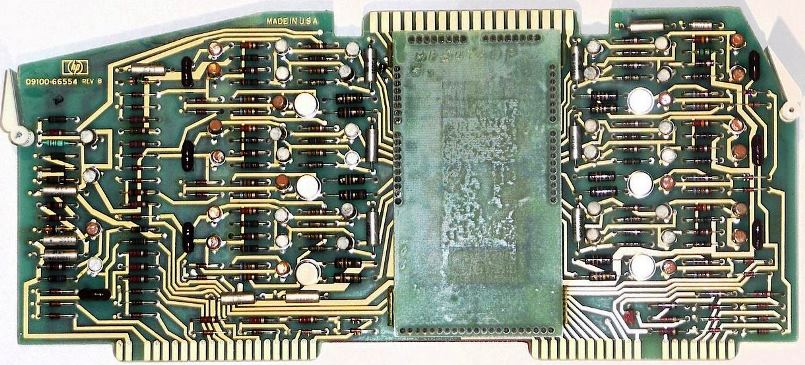
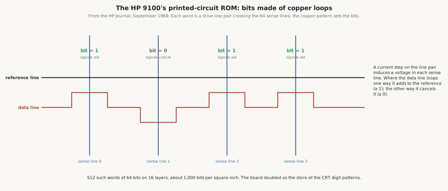
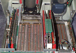
The program ROM holds 512 words of 64 bits, 32,768 bits in all: the subroutines, the constants, the character encoders, and the patterns that draw the digits on the tube. It is not a chip but a 16-layer printed circuit board. Each word is a pair of drive lines, a reference line and a data line, running across 64 sense lines. A current step on the pair induces a pulse in every sense line it crosses; where the data line has been routed so that its signal adds to the reference, the sense amplifier reads a 1, and where it cancels it, a 0. The bits are literally the shape of the copper, at about 1,000 bits to the square inch. Chuck Near designed the board, and HP’s printed-circuit shop had to learn to etch 10-mil lines where 50 mils was the norm.
The control ROM is a core rope, “a wire braid toroidal core read only memory” in the HP Journal’s words, of 64 words of 29 bits. A trapezoidal current pulse through one of 64 word wires passes through some of 29 ferrite toroids and not others; each toroid it threads acts as a transformer and turns on an output transistor. The control ROM can modify its own address, so it runs short micro-sequences, such as unpacking a stored constant. Six bits of each 64-bit program word choose one of its 64 words; the rest carry a condition code and two 9-bit next addresses, between which the machine branches according to the condition. Between three and seven operations run in parallel at each step.
5.1.3 The core memory
The working memory is magnetic core: 2,208 bits, arranged as 23 registers of 16 digits of 6 bits. Three are the display registers X, Y and Z, sixteen are the user’s storage registers, and four are hidden. A 6-bit digit holds a BCD digit, a sign or a blank, or one program step, so a storage register holds 14 program steps and the 16 registers hold 196. The cores are a wide-temperature lithium ferrite, the drivers have temperature-compensated current sources, and special circuits protect the data at power-off and power-on: the 9100 remembers its registers and its program when it is switched off. The 9100B has 3,840 bits.
5.1.4 Numbers and algorithms
Cochran’s article explains the arithmetic. A number has a 12-digit mantissa, of which 10 are displayed and 2 are guard digits, and a 2-digit exponent, covering 10⁻⁹⁸ to 10⁹⁹.
- Addition aligns the exponents by offsetting the digit positions rather than shifting the numbers.
- Multiplication adds the multiplicand once for each unit of each multiplier digit, shifting between digits; division subtracts until overdraft, restores, and moves on, as on a mechanical calculator.
- Square root is a pseudo-division based on the sum of odd numbers, as fast as a division and accurate to one part in 10¹⁰.
- Trigonometric functions use an iterative rotation of coordinate axes after reducing the angle to less than one radian; the core routine finds the tangent and the sine and cosine follow from identities, which keeps all 12 digits even for tiny angles. Logarithms and exponentials use a “compound iteration” of pseudo-multiplication and pseudo-division. These are the methods of Jack Volder’s CORDIC and J. E. Meggitt, brought to the project by the consulting mathematician Malcolm McMillan.
HP’s times: addition 2 ms, multiplication 22 ms, division 27 ms, square root 30 ms, logarithm 130 ms, a trigonometric function about 330 ms.
5.1.5 Keyboard, card and display
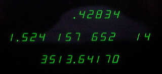
Each of the 63 keys works one gold-contact switch, and a matrix encodes the key as six data lines plus a strobe, delayed for contact bounce, with an interlock against two keys at once. The magnetic card has four tracks at 200 bits per inch: each 6-bit program step is split into two 3-bit halves across three tracks, and the fourth is the strobe. The display draws its E- and I-shaped sweeps, described in the previous volume, on a flat-faced electrostatic tube about 11 inches long, behind a dark filter that light from the room must pass through twice and the image only once. The tube’s unusually wide deflection angle makes its linearity poor, and it is the one part of a 9100 that cannot be replaced.
5.2 The Victor 3900: a calculator on MOS chips
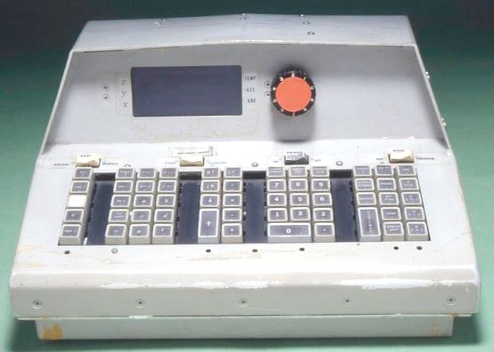
The Victor 3900 was designed by General Micro-electronics around its own p-channel MOS integrated circuits. The main board carries 29 chips of 23 types, with about 250–300 transistors each; a dual 48-bit dynamic shift register chip, used seven times, holds the registers. Each register is 22 BCD digits long (20 digits, sign and decimal position), and there are seven: three working registers, two memory accumulators shown on the screen, a temporary register and a hidden store. How 22 four-bit digits fit into 48-bit registers is not explained in the museum’s account, which notes the puzzle itself.
The registers recirculate, like a delay line, but in silicon: a dynamic shift register stores each bit as charge on the gate of a MOS transistor and passes it along on two non-overlapping clock phases (Robert Norman’s patent US 3,454,785). The adder is a single bit-serial full adder with a carry flip-flop, and the digits are coded in excess-three. Leading zeros are suppressed by comparing each digit with the ones before it (US 3,388,384).
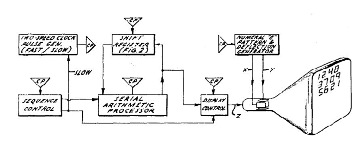
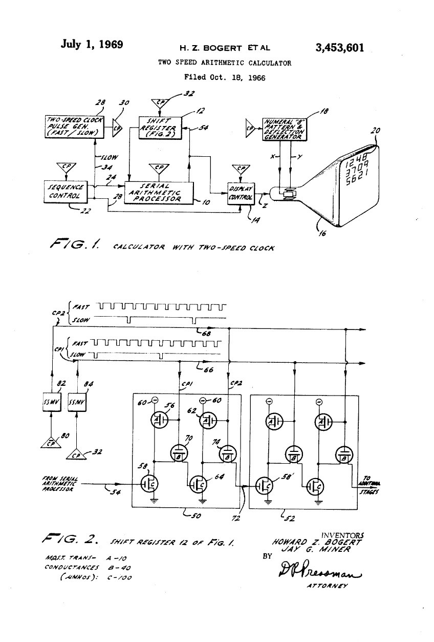
The clock has two speeds, the subject of Howard Bogert and Jay Miner’s patent US 3,453,601: 330 kHz while calculating, so that every operation finishes within 400 ms, and 60 kHz while displaying, just fast enough to avoid flicker, which cuts the power from 30 W to 20 W.
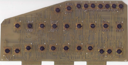
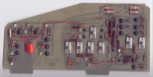
The chips were spot-welded to the boards, which makes repair at chip level very hard, and the machine suffered from static discharge through the keyboard and from power-on surges: an unlucky moment of switch-on could over-volt the logic supply, and that is how all 25 prototypes were lost. A 1965 Friden report on the 3900 is in the Library.
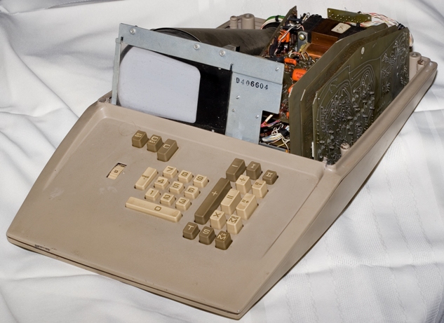
5.3 The Wyle Scientific: drum, then wire
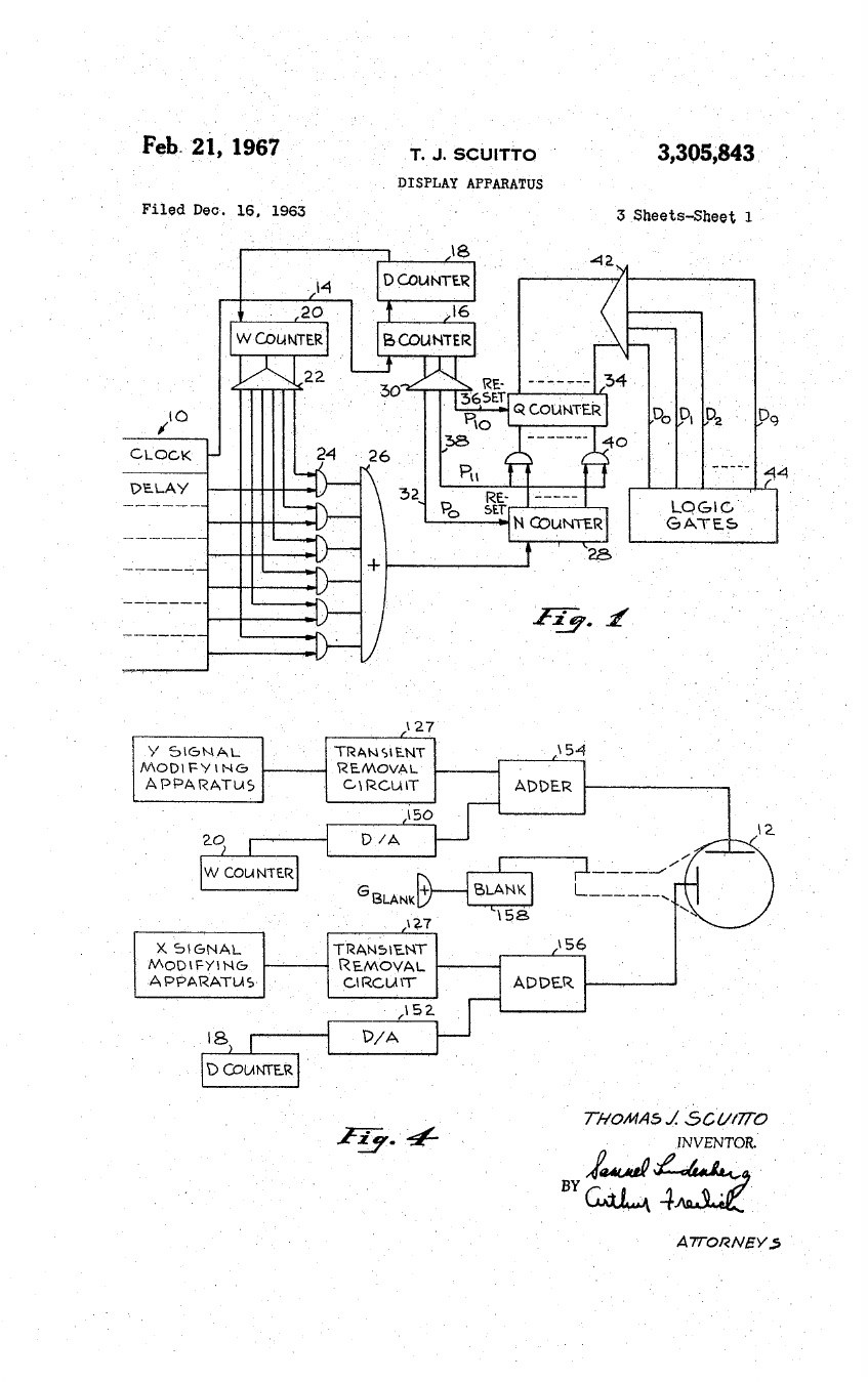
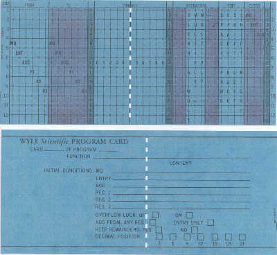
The Wyle WS-01 kept its six registers and its timing on a home-built rotating magnetic disk of about 1,700 bits with six register tracks and a clock track; the WS-02 replaced it with a Digital Devices magnetostrictive delay line. Its logic is discrete germanium transistors, mostly 2N404, in resistor-transistor logic. Scuitto’s display patent shows how the timing worked: a modulo-12 bit counter divides each digit into twelve positions, nine of which carry the digit as a count of pulses, as in the Friden. A digit counter and a register counter select the place and the line, and a pulse counter tallies the pulses of each digit and decodes them, one of ten, to choose the arcs that draw it.
5.4 The SCM Cogito 240
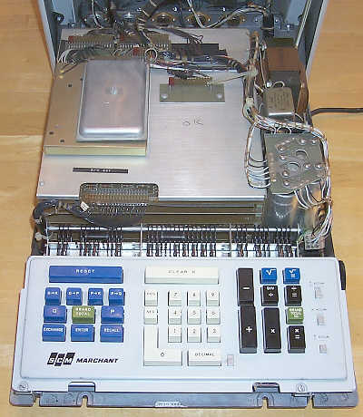
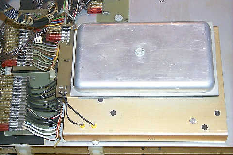
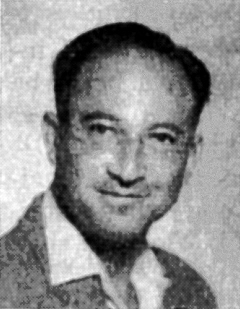
Stanley Frankel’s Cogito is all discrete diode-transistor logic, bit-serial BCD at about 1 MHz, with three working registers (K, P and Q) and three shadow registers, all in a Digital Devices delay line of 480 bits with a delay of 460 µs. Frankel’s patent on recirculating-memory timing is US 3,518,629. Six logic boards of about 9 × 10 inches and the deflection, scan and blanking boards stack in the clamshell cabinet.
5.5 The integrated-circuit Fridens: 1160, 1162 and 1166
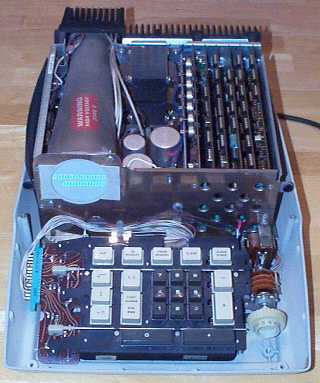
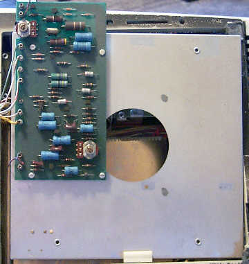
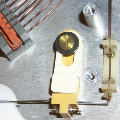
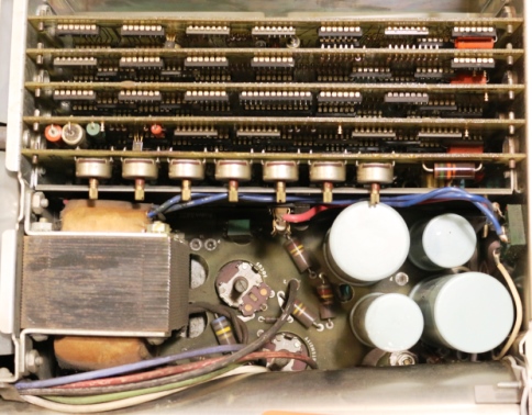
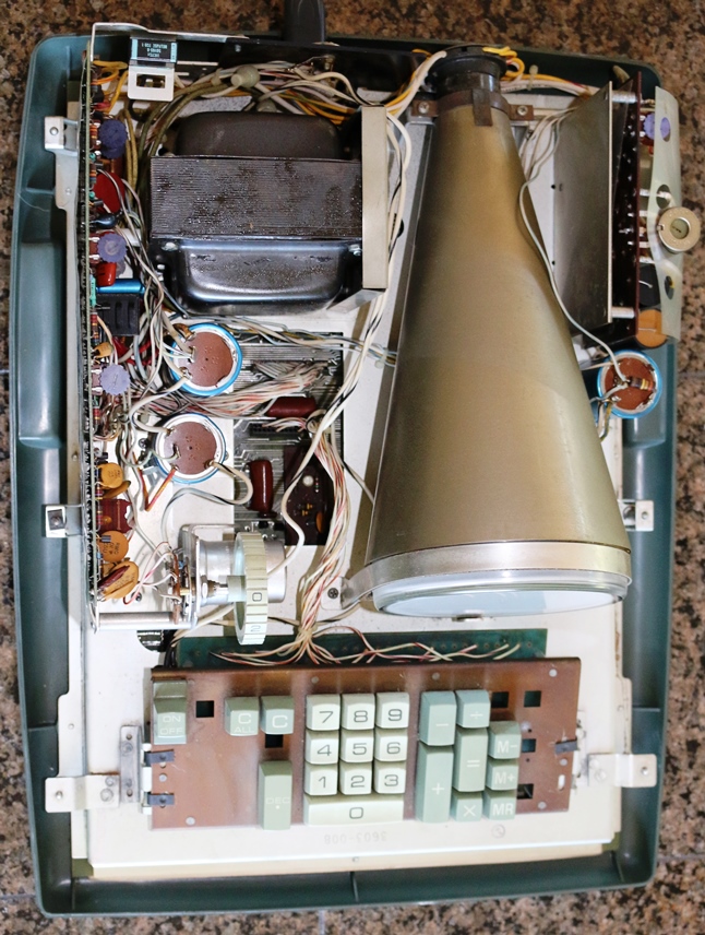
The 116x machines are the EC-130 and 132 rebuilt with integrated circuits, keeping the architecture: a delay line, the A, C and D counters (now custom Texas Instruments chips SN1286, SN1287 and SN1288), and a figure-8 stroke display. The delay line is about 40 feet of thinner beryllium-copper wire with a 4 ms delay and a single nickel tape at each transducer. The logic is TI SN158xx diode-transistor-logic ICs with Fairchild and Motorola equivalents and 7473/7474/7476 TTL flip-flops: 83 ICs in the 1160, 93 in the 1162 on six boards, and 105 in the 1166. A 2.8 MHz oscillator divided by four gives the 1162’s 700 kHz master clock. Board 1 generates the display with two custom SN9095 chips and discrete parts, and an analog board beside the tube holds the deflection amplifiers and beam drive; the 3 kV supply for the 3WP1 tube is on the backplane. The 1162 logic schematic is in the Library.
5.6 The Victor 14-321
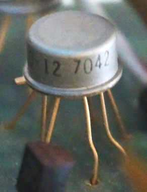
The Victor 14-321 shows the transition in one model. Its 114 DTL integrated circuits, clocked at 2 MHz for a 1 MHz bit rate, first stored their registers in a 412 µs magnetostrictive delay line. From late 1969 Victor replaced the line with two 200-bit MOS shift-register chips, the memory technology that was about to make the delay line, and with it the CRT, obsolete.
5.7 Documents
- HP: HP Journal, September 1968; 9100B schematics; 9100B microprogram flowcharts; Trinity College Dublin catalogue; Osborne’s story; patents US 3,566,160, US 3,623,156, US 3,588,873.
- Victor 3900: patents US 3,453,601, US 3,388,384, US 3,454,785; Friden’s 1965 report.
- Wyle: display patent US 3,305,843; instruction manual.
- Cogito: US 3,518,629.
- Friden 116x: 1162 logic schematic.
Comments (0)